The NT99141 chip is a 1/4-inch high-definition CMOS image sensor. The complete technical data sheet of the chip provides detailed technical specifications, functional descriptions and application circuits, and is an important reference for engineers and technicians who design and develop products based on this image sensor. The following is a detailed description of the main knowledge points of the chip:
1. Chip Features
Chip features refer to the core technical parameters and functional highlights of the CMOS image sensor, such as the sensor's resolution, dynamic range, low-light performance, frame rate, and specific image processing functions related to it.
2. Key Performance Indicators
Describes the key performance parameters of the NT99141 chip, such as sensitivity, signal-to-noise ratio, dynamic range, power consumption, and temperature characteristics, which are important indicators for determining whether the image sensor meets the performance requirements of specific application scenarios.
3. General Description
The general description contains basic information about the chip, such as purpose, imaging principle, size specifications, pin definition, etc.
4. FUNCTION DESCRIPTION
The various functions of the NT99141 sensor are explained in detail, including pixel array, default readout order, analog gain control, 10-bit analog-to-digital converter, image windowing, output format, special effects, gamma correction, and luminance accumulation mode.
5. CONTROL REGISTERS
This section lists in detail the various registers used to control the image sensor and their functions, for example:
– Sensor Control Registers (0x3000) are used to set the basic parameters of the sensor;
– SOC Control Registers (0x3200) are used to set system-level configurations, such as system clock, system operation, etc.;
– SOC Lens Shading Correction Registers (0x3210) are used to correct the chromatic aberration of the lens;
– SOC Statistic Registers (0x3250) are used to obtain statistical information in the image sensor;
– SOC Gamma Registers (0x3270) are used to adjust the gamma of the image.
6. TWO-WIRESERIAL INTERFACE BUS
Describes how to configure and control the NT99141 chip through a two-wire serial interface. This section lists in detail the timing and methods of single read from random location (SingleReadfromRandomLocation), single read from current location (SingleReadfromCurrentLocation), continuous read start position setting, single write and continuous write and other related operations.
7. JPEG output timing (JPEG OUTPUT TIMING)
Detailed description of how to handle the output timing requirements of image data in JPEG output mode.
CCIR656 OUTPUT TIMING
Describes the timing of the CCIR656 standard output of the NT99141 chip to support video encoding formats that comply with this standard.
9. PIN CONFIGURATION & PACKAGE OUTLINE
Detailed description of the physical pin arrangement of the NT99141 chip and the package dimensions, providing the necessary physical reference for circuit board design and chip installation.
10. REFERENCE CIRCUIT
A reference circuit design is provided to help engineers understand how to integrate the NT99141 chip into a specific product design and ensure that the image sensor can work properly.
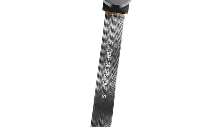
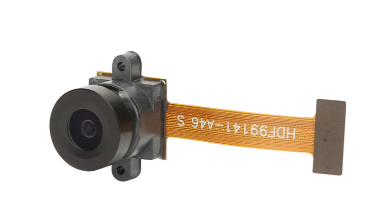
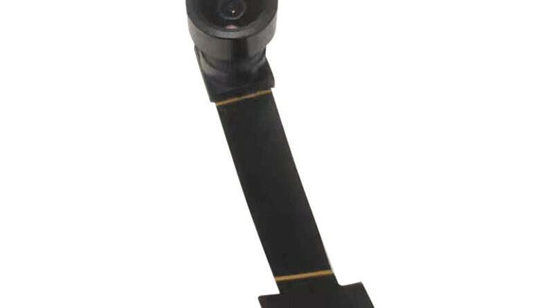
Dogoozx NT99141 camera module recommendation:
-
Dogoozx 720P HD Wide Angle with JPEG QR code barcode scanning DVP NT99141 Camera Module
-
Dogoozx 720P with JPEG DVP NT99141 Pinhole lens temperature measurement Camera Module
-
Dogoozx Customized 1MP NT99141 720P self-with JPEG image recognition DVP Camera Module


