1. Introduction to camera module
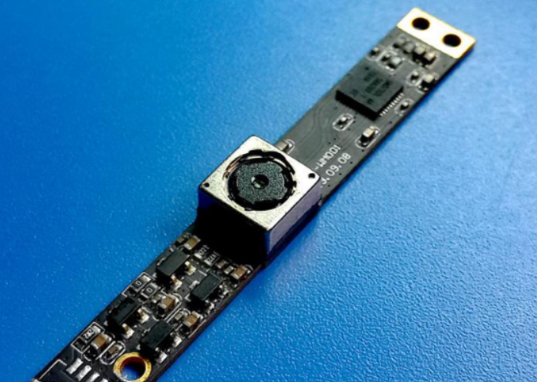
Camera module , full name Camera Compact Module, abbreviated as CCM. CCM includes several major parts: lens, voice coil motor (VCM), sensor, flexible circuit board (FPC), image processing chip (DSP).
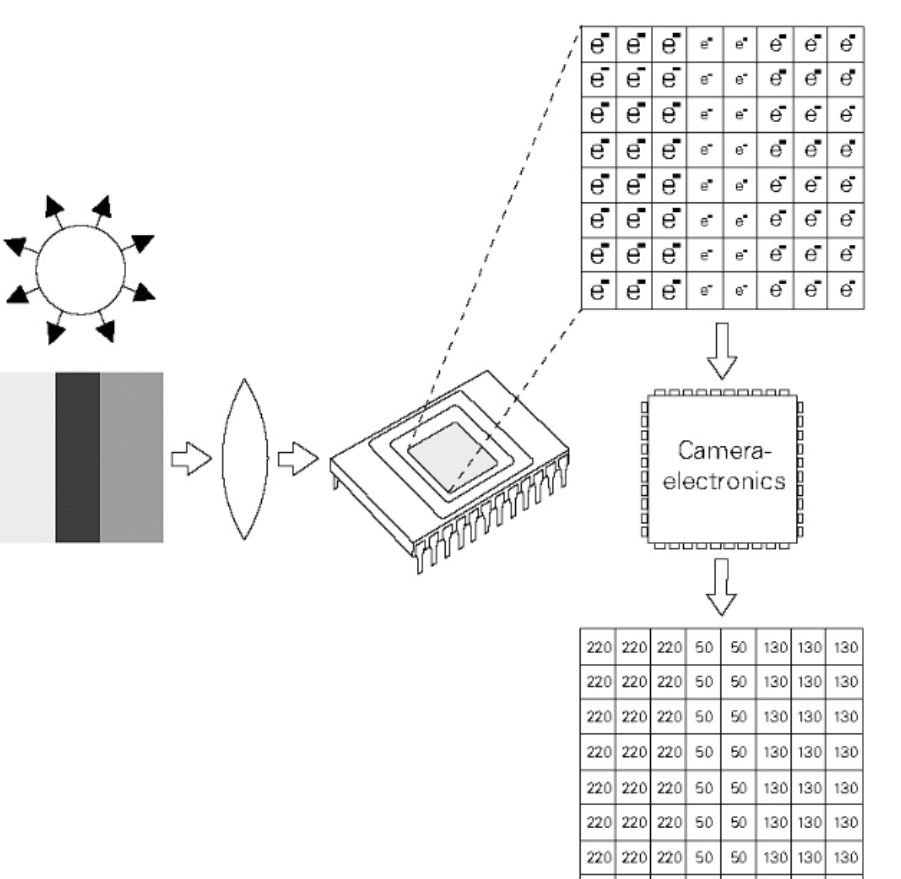
Working principle: The light gathered by the object through the lens is converted into an electrical signal through the CMOS or CCD integrated circuit, and then converted into a digital image signal through the internal image processor (ISP) and output to the digital signal processor (DSP) for processing and conversion into a standard GRB, YUV and other format image signal.
The camera module mainly consists of the following parts:
Lens: Focuses light onto the image sensor.
Voice coil motor (VCM): Completes the camera's autofocus.
IR-cut filter: Filters out invisible light to the human eye.
Image sensor: Converts light signals into electrical signals.
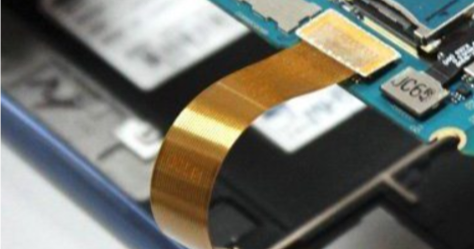
Flexible printed circuit board (FPCB): Connects the camera module to the main processor and transmits data.
The following figure shows the structure of several core components of a common mobile phone camera module.


2. Composition
1. Lens
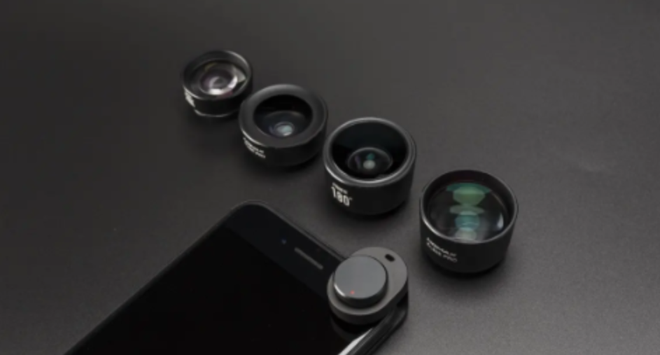
The main function of the lens is to converge the light collected from the outside world onto the image sensor. The principle is pinhole imaging. With different lenses, the light is focused onto the photosensitive chip at the bottom of the lens (that is, the sensor) to form

Modern lenses are generally composed of several lenses to achieve more complex imaging effects. Lenses are divided into glass and plastic materials. For example, 2G2P means that this set of lenses is composed of two glass lenses and two plastic lenses. Generally, glass lenses have better imaging effects and are more expensive.

2. VCM (Voice Coil Motor)
The full name is Voice Coil Motor, which is a type of motor in electronics. Because the principle is similar to that of a speaker, it is called a voice coil motor, which has the characteristics of high frequency response and high precision. Its main principle is to control the stretching position of the spring sheet by changing the DC current of the coil in the motor in a permanent magnetic field, thereby driving the up and down movement. Mobile phone cameras widely use VCM to achieve the autofocus function. The position of the lens can be adjusted through VCM to present a clear image.
A coil is placed in a permanent magnetic field. When the coil is energized, a magnetic field will be generated (Ampere's law), which will generate attraction or repulsion with the peripheral permanent magnet, causing the coil to move under force. If the lens is placed on the coil, the coil can be driven to move back and forth by changing the current size, thereby controlling the position of the lens and completing the focusing function.
VCM is usually used with VCM Driver IC (VCM driver chip) and AF (Auto Focus) algorithm. First, the image collected by the Sensor is input into the ISP, and the AF algorithm in the ISP calculates the focus steps of the current image and transmits it to the Driver IC through I2C. The Driver IC calculates the current required to move the coil to that position, thereby accurately controlling the behavior of the lens to achieve the effect of autofocus. Of course, this method can also achieve the effect of Optical Image Stabilizer (OIS), and the principle is the same.


VCM Performance Indicators
The performance of VCM mainly depends on the ratio of current to travel distance. Starting from the starting current, the current rise must be proportional to the travel distance that can be driven. The smaller the required rising current, the higher the accuracy. At the same time, it also depends on the maximum power consumption, maximum power, and size.
VCM classification
Structurally, they can be divided into three categories: (1) spring-type structure; (2) ball-type structure; (3) friction type structure.
Based on their functions, they can be roughly divided into five categories: (1) Open loop motor; (2) Close loop motor; (3) Alternate motor; (4) OIS optical image stabilization motor (divided into translation type, tilt-shift type, memory metal type, etc.); (5) OIS+Close loop six-axis motor.
AF principle
After entering the auto focus mode, the Driver increases from 0 to the maximum value, causing the lens to move from its original position to the maximum displacement. At this time, the sensor imaging surface automatically takes pictures and saves them in the DSP. The DSP calculates the MTF (Modulation transfer function) value of each picture through these pictures, and then finds the maximum value in this MTF curve. Through the algorithm, it obtains the current size corresponding to this point, and once again instructs the Driver to provide this current to the voice coil, so that the lens is stabilized on this imaging surface, so as to achieve automatic focus.
Zoom and focus
A: To achieve optical zoom, a zoom motor (ZOOM) is used
By moving the lens inside the lens to change the position of the focus, changing the focal length of the lens, and changing the angle of view of the lens, the effect can be magnified or reduced.
B: Auto focus using focus motor (AF)
By moving the position of the entire lens (rather than the lens inside the lens) at a micro distance, the focal length of the lens is controlled to achieve clear images. This is a common method used in mobile phones.
Optical focus and optical zoom are different concepts:
Optical zoom is to change the focus position by moving the relative position of the lens inside the lens, changing the length of the lens focal length, and changing the angle of view of the lens, thereby achieving image magnification and reduction;
Optical focus actually adjusts the position of the entire lens (rather than the lens inside the lens) to control the image distance, thereby making the image clearest.
3. Infrared filter
The function of the IR-cut filter is to filter out infrared light. The wavelength range of light that the human eye and electronic photosensitive devices can sense is different. The wavelength range of light that electronic photosensitive devices can sense is much larger than that of humans. Therefore, it is necessary to filter out the light that the human eye cannot sense to prevent them from causing color cast and ripple phenomena and improve color reproduction. This will have a great impact on the subsequent ISP tuning work.
IR-cut filters are divided into two categories: ordinary IR and blue glass IR. The former reflects infrared and ultraviolet light, preventing them from entering the sensor, while the latter absorbs infrared and ultraviolet light, preventing them from entering the sensor. The former easily causes multiple reflections of infrared light, resulting in shading and causing large color differences in the final imaging effect. Although the latter does not have this problem and has better effects, its cost is also ten times that of the former.
4. Image Sensor
The image sensor is the core component of the entire module and the focus of this introduction. It is a semiconductor chip with hundreds of thousands to millions of photodiodes on its surface. These photodiodes will generate charges when exposed to light, thereby converting the light signals collected by the lens into electrical signals. Therefore, if the role of the lens is equivalent to the lens of the human eye, then the role of the sensor is similar to the retina, and the photosensitive diodes on the sensor are the visual cells on the retina.
The sensor is mainly used to convert the collected external light signals into electrical signals for subsequent electronic systems to process and store. The sensor's photosensitive units, that is, each pixel unit, are arranged into a pixel array with photosensitive diodes distributed on it. After being stimulated by external light, these diodes will generate electrical signals of different strengths according to the light intensity, and then be discretized into digital signals through internal A/D conversion.

A photodiode can be roughly regarded as a capacitor. The stronger the light, the more charge accumulates on the capacitor at the same time, and the greater the voltage generated. If the voltage across the capacitor is converted into a digital signal through A/D, a digitized value can be obtained, and all the pixels can be combined to obtain a grayscale image. The stronger the light, the larger the value, and the closer the pixel is to white; the weaker the light, the smaller the value, and the closer the pixel is to black. This is consistent with our usual cognition.
According to the different types of photosensitive diodes, the widely used sensors on the market can be divided into two categories: CCD Sensor and CMOS Sensor. CCD is Charge Coupled Device, that is, charge coupled device; CMOS is Complementary Metal Oxide Semicondutor. The specific photosensitivity principles of the two semiconductors are not the focus of this article and will not be discussed in detail. At present, CMOS Sensor has basically replaced the position of the past CCD Sensor due to its advantages of lower power, faster processing speed and lower manufacturing cost, especially in the field of mobile phones and mobile devices. However, the advantage of CCD Sensor is that it performs better in low light conditions, is not affected by digital noise like CMOS, and does not rely so much on the denoising work of ISP.
Image sensor is a semiconductor chip with millions to tens of millions of photodiodes on its surface. When the photodiodes are exposed to light, they will generate electric charge and convert the light into electrical signals. Its function is similar to that of human eyes, so the performance of the sensor will directly affect the performance of the camera .
4.1 Sensor Structure

4.2 Classification
Photosensitive element: CCD, CMOS (PPS and APS)
Different processes: front-illuminated FSI, back-illuminated BSI, stacked
4.3 Indicators
1. Pixels
There are many photosensitive units on the sensor, which can convert light into electric charge to form an electronic image corresponding to the scene. In the sensor, each photosensitive unit corresponds to a pixel. The more pixels, the more details of the object it can sense, so the clearer the image is. The higher the pixel, the clearer the imaging effect. The product of the camera resolution is the pixel value, for example: 1280×960=1228800
2. Target size
The size of the photosensitive part of the image sensor is generally expressed in inches. Like a television, this data usually refers to the diagonal length of the image sensor, such as 1/3 inch. The larger the target surface, the better the light transmission, while the smaller the target surface, the easier it is to obtain a larger depth of field.
3. Light sensitivity
That is, the intensity of incident light is sensed through CCD or CMOS and related electronic circuits. The higher the sensitivity, the more sensitive the photosensitive surface is to light, and the higher the shutter speed, which is especially important when shooting moving vehicles and night monitoring.
4. Electronic shutter
It is a term proposed in comparison with the mechanical shutter function of a camera. It controls the photosensitivity time of the image sensor. Since the photosensitivity value of the image sensor is the accumulation of signal charge, the longer the photosensitivity, the longer the signal charge accumulation time, and the greater the amplitude of the output signal current. The faster the electronic shutter, the lower the sensitivity, which is suitable for shooting under strong light.
5. Frame rate
Refers to the number of pictures recorded or played per unit time. Playing a series of pictures continuously will produce an animation effect. According to the human visual system, when the picture playback speed is greater than 15 pictures/second (i.e. 15 frames), the human eye can hardly see the picture jumping; when it reaches between 24 pictures/s and 30 pictures/s (i.e. 24 to 30 frames), the flicker phenomenon is basically unnoticeable.
Frames per second (fps) or frame rate indicates how many times per second the graphics sensor can update when processing a field. A higher frame rate results in a smoother, more realistic visual experience.
6. Signal-to-Noise Ratio
It is the ratio of signal voltage to noise voltage, and the unit of signal-to-noise ratio is dB. Generally, the signal-to-noise ratio value given by the camera is the value when AGC (automatic gain control) is turned off, because when AGC is turned on, it will enhance the small signal, so that the noise level will also increase accordingly.
The typical value of signal-to-noise ratio is 45-55dB. If it is 50dB, the image has a small amount of noise, but the image quality is good; if it is 60dB, the image quality is excellent and there is no noise. The larger the signal-to-noise ratio, the better the control of noise. This parameter is related to the number of noise points in the image. The higher the signal-to-noise ratio, the cleaner the picture feels, and the fewer point-shaped noise points there are in the night vision picture.
4.4 ISP
4.4.1 RAW DATA
The sensor converts the light transmitted from the lens into an electrical signal, and then converts it into a digital signal through the internal AD. Since each pixel of the sensor can only sense R light, B light, or G light, each pixel stores monochrome data at this time, which we call RAW DATA data. To restore the RAW DATA data of each pixel to the three primary colors, ISP is required to process it.
4.4.2 ISP Processing
ISP (Image Signal Processing) is mainly responsible for processing digital images and converting the raw data collected by the sensor into a format supported by the algorithm.
Specific process:
1. After the external light passes through the lens, it is filtered by the color filter and then shines on the sensor surface;
2. The sensor converts the light transmitted from the lens into an electrical signal, and then converts it into a digital signal through the internal AD.
3.1. If the sensor does not integrate ISP, it directly transmits the baseband through the transmission line (baseband is the basic frequency band, see "Communication Principles" for details; the other is mode modulation transmission), and the data format at this time is RAW DATA.
3.2. If ISP is integrated, RAW DATA data is processed by AWB (automatic white balance), color matrix, lens shading, gamma, sharpness, AE (automatic exposure control) and de-noise, and then outputs data in YUV or RGB format.
4.4.3 "Communication Principles" – Baseband
The full name of baseband in English is Baseband, which can also be translated as the frequency band (frequency bandwidth) inherent in the original electrical signal sent by the "source" (information source, also known as the transmitting terminal) without modulation (spectrum shifting and transformation), called the basic frequency band, or baseband for short. Baseband corresponds to frequency band, frequency band: the frequency bandwidth occupied by the baseband signal before modulation (the difference from the lowest frequency to the highest frequency occupied by a signal).
5 、DSP
Digital signal processor DSP (DIGITAL SIGNAL PROCESSING) function: mainly through a series of complex mathematical algorithms, to optimize the parameters of digital image signals, and the processed signals through USB and other interfaces to PC and other devices
Difference between DSP and ISP
Glossary:
ISP is the abbreviation of Image Signal Processor, which is image signal processor.
DSP is the abbreviation of Digital Signal Processor, which is a digital signal processor.
Functional explanation:
ISP is generally used to process the output data of Image Sensor, such as AEC (Automatic Exposure Control), AGC (Automatic Gain Control), AWB (Automatic White Balance), color correction, Lens Shading, Gamma correction, bad pixel removal, Auto Black Level, Auto White Level, etc. (For details, please visit: https://blog.csdn.net/djfjkj52/article/details/115324741 for explanation of "Camera automatic exposure, auto focus, automatic white balance, ISP, image processing and color model, color space")
DSP has more functions. It can take photos and display them (JPEG encoding and decoding), record and play back (Video encoding and decoding), H.264 encoding and decoding, and many other processing functions. In short, it processes digital signals.
6. Flexible printed circuit board
The main function of the Flexible Printed Circuit Board (FPCB) is to connect the components to the main processor and complete the original data transmission function between the sensor and the main processor.


7. The imaging process of mobile phone cameras
Mobile phone camera link

Let's first take a look at the overall link of the mobile phone camera. There are 5 steps in total. This article will explain the first 3 parts (hardware part):
Camera Lens : The camera lens of a mobile phone. Light passes through the lens and reaches the COMS image sensor.
Image Sensor : The CMOS image sensor converts the light signal into an electrical signal, and then converts it into a digital signal through the internal ADC.
ISP : The digital signal is transmitted to the ISP for processing, mainly for correction, white balance, exposure control, etc.
SOC : This step is at the application layer (such as App). The image data is post-processed by the CPU and GPU, such as adding filters, etc.
Display : Finally, the image data is displayed on the screen


